A New Angle for Quantum
Electrical and computer engineers are working to scale production of quantum devices with etching method in silicon carbide
Photons, or particles of light, are like a quantum notepad. With these infinitesimal dots of energy, quantum devices store quantum information.
Color centers are the essential hub for photons in quantum devices. They are the components that emit and maintain photons, functioning as a quantum memory bank. However, they are challenging to fabricate, particularly for the industrial development of quantum technology.
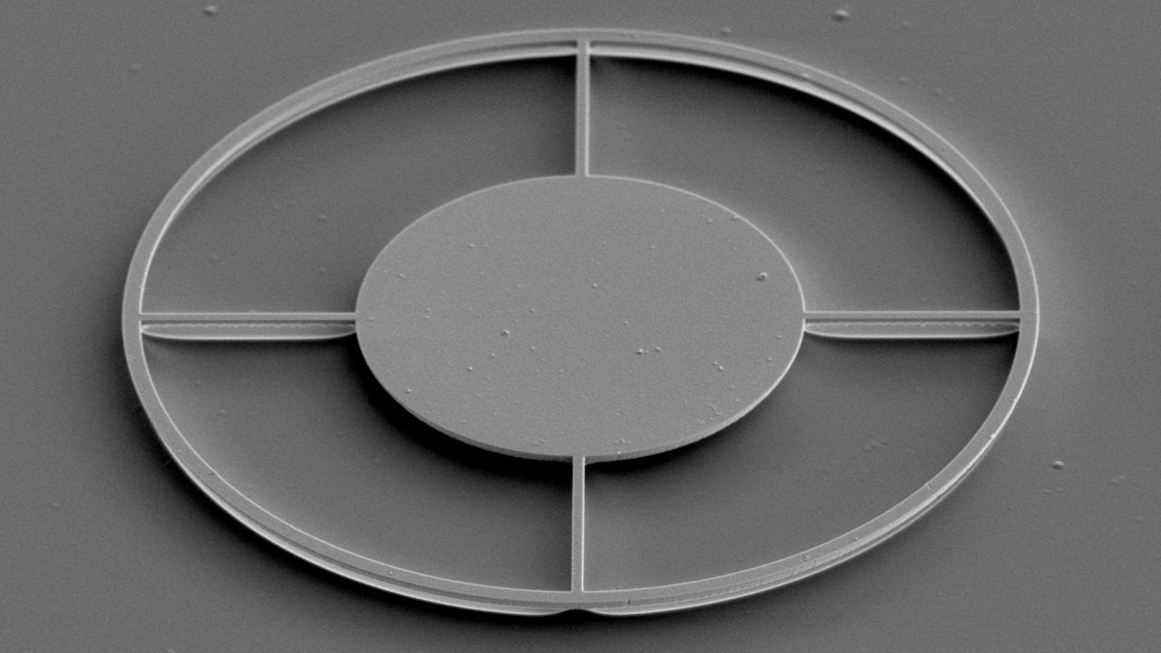
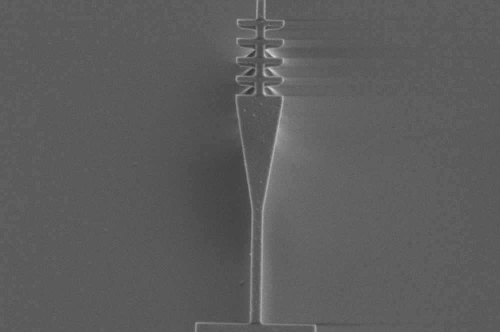
At the University of California, Davis, researchers have demonstrated an angle etching method for fabricating quantum photonic devices at the wafer scale in silicon carbide. This development has brought within reach the reality of producing hardware like quantum nanodevices at scale and, thus, the development of the quantum internet.


Associate Professor of Electrical and Computer Engineering Marina Radulaski led the effort; her graduate student Sridhar Majety, who received his Ph.D. in quantum nanophotonics from UC Davis in 2024, was the first author of the corresponding paper, published in Springer’s npj Nanophotonics journal.
Light Suspension
Suspended photonics with color centers embedded within are a type of technology that helps carry light in quantum hardware.
The prevailing technique for creating these devices in silicon carbide has been stacking two materials and then selectively removing parts of one material to achieve the “suspension” required for the color center to function. This technique is useful for creating devices with color centers for small chips but not at the larger, more complicated scale typical in the semiconductor industry.
“Historically, people would stick silicon carbide to bulk materials and then polish the topmost layer to be very thin, like a couple of microns thick,” Majety said, explaining how engineers manufacture photonics with color centers. “However, these classical techniques were deteriorating the properties of the color center we use for quantum communications and quantum photonics.”
A Material Difference
To address this deterioration issue, Radulaski and her team found inspiration from a project conducted at Harvard over 10 years ago. That team demonstrated an etching method for suspended photonics capable of removing finer layers of material than polishing.
“They used something called angle etch,” Majety said, “which is basically a dry etch process in which etching ions bombard the material at an angle from all directions to reach underneath the surface layer. This creates a suspended structure in the bulk material that resembles the shape of Toblerone chocolate."

The Toblerone-like structure maintains the intrinsic composition of color centers without deteriorating their quantum properties, explained Radulaski. This is because color centers depend on specific organizations of atoms in a crystal, which processing methods can ruin.
“Say you want to cut a princess diamond shape using a big axe. It wouldn’t work. Or you try to keep egg liquid while boiling it in hot water for half an hour: It would change shape and turn to solid,” Radulaski said.
The thing is, the Harvard team created their suspended photonics in diamonds, a material inappropriate for industrial applications of color centers due to its high price. Furthermore, diamonds are tough to source in the wafer shape quantum devices require.
“The proof of concept was there,” Majety said. “But as an engineer, you always think about the question, ‘Can we manufacture this at scale?’”
With this angle etching method in their toolkit and question in mind, Radulaski’s team turned to silicon carbide, an inexpensive material widely available for electronics production. They conducted experiments at the College of Engineering’s cleanroom, the Center for Nano-MicroManufacturing, and replicated in silicon carbide wafers the suspended photonics the Harvard team had made in diamond.
“Color centers in silicon carbide are formed when a nitrogen particle and an atomic vacancy occupy spots of neighboring carbon and silicon sites in the crystal,” Radulaski said. “These systems emit near-infrared light suitable for use in optical fiber and to store quantum information for a relatively long time, sufficient to execute quantum operations.”
Scaling the Future
The next steps are to test this method further and translate it for industrial applications to produce quantum devices at scale.
“The wafer-scale nanofabrication process we developed in silicon carbide is going to enable the production of complex quantum optical circuits and multiple identical devices on the same sample, just like how processors are made for today’s computers,” Radulaski said. “The hope is that this will allow us to perform new quantum computations and enable identically-performing elements across a quantum network.”
While these quantum devices and the quantum internet they make possible may not arrive soon, their arrival is closer than ever.
"This experiment doesn't make quantum internet realizable in the next couple of years,” Majety said, “but it's a very important demonstration showing it is possible to economically make suspended photonics on wafers. That's the most important outcome of this project: that you can make these things at scale because everyone's been struggling to do that.”
Due to the strength of this project, Majety won the electrical and computer engineering department’s Richard and Joy Dorf Graduate Student Award, which recognizes a student’s promise for outstanding intellectual contributions. Another co-author on the paper and current graduate student in Radulaski’s lab, Pranta Saha, won a poster prize award for a demonstration of the team’s findings at the 816. WE-Heraeus-Seminar in Bad Honnef, Germany.


